The ISR would initially be servicing only two interrupt sources: the NXP 2692 DUART and the Dallas DS1511Y watchdog timer (WDT). The DUART would be generating interrupt requests (IRQ) when a byte was received and when it was able to accept a byte for transmission. Serial communications works best when buffers are used, especially for reception, as there may be occasions when the incoming data flow can't be immediately processed by the program expecting it. Buffering transmission is also beneficial, as the MPU can write data to the DUART much faster than the latter can transmit it. If transmission is not buffered then the whole system will be slowed down to the character reception rate of the remote device, even when small amounts of data are to be transmitted.
Since the DUART has two communication channels, a total of four buffers are required. Initially, I settled on a 256 byte buffer size, because maintaining the buffer read/write indexes would be very simple (they would wrap to zero when the end of a buffer is reached). Later on, I reduced each buffer's size to 128 bytes, thus reducing BIOS memory consumption (a change that had no perceptible effect on performance). As I noted on the previous page, I have quite a bit of experience with the DUART's operation, so I didn't anticipate any particular problems in writing a driver for it.
In the case of the watchdog, although it is a complete timekeeper, with a 24 hour clock (with alarm) and a calendar, its only job at this stage of development would be to generate a jiffy IRQ at 10 millisecond intervals. Processing a jiffy IRQ would result in the incrementing of a 32 bit uptime counter and the decrementing of a 16 bit down counter, the latter which could be used to generate programmable time delays. Also, the jiffy IRQ would be used for a short-term delay function needed to properly program some of the DUART registers. The initial test firmware had generated the needed delays with a busy loop (aka "spin loop"). Doing it with IRQs would produce more predictable performance and would ultimately require a bit less code.
Unlike the DUART, the watchdog was new hardware to me, so I expected some difficulty in getting it to work properly, and I wasn't disappointed. The problem lies more with the clarity of the part's data sheet than anything else—it certainly isn't due to any deficiency in the parts themselves, which are very high quality. Dallas Semiconductor, the manufacturer of the watchdog, has never been noted for particularly lucid data sheets. The DS1511Y's data sheet has admirably carried on that tradition, more because of what it has omitted than what it has said. The buyout of Dallas by Maxim didn't help much, but at least technical support was improved—I got a response within a few hours of contacting Maxim via E-mail.
Firmware development for a newly-designed system can be a tedious and cumbersome process, as each iteration—written in assembly language, of course—must be burned into a ROM, followed by the ROM being plugged into the computer for testing. Complicating the process is the necessity of writing compact code to avoid running out of ROM space. Further complicating matters is that debugging is often accomplished by inference, as a bug may cause total system fatality, leaving few clues as to the nature of the error. This means a thorough understanding of what is supposed to happen is required, since a crash may not display anything of value on the screen. Once the problem has been identified and the code has been reassembled, a new ROM must be burned and the cycle repeated until all bugs have been found and eliminated. Unlike high level language development, writing firmware for "bare metal" is unforgiving in nature. This is a case where a disciplined and structured approach to software development pays off. Lots of patience helps as well.
It took several weeks to write the basics. The BIOS part of the ROM not only includes the BIOS proper, it has a reset handler, ISR, and chip setup data tables. In particular, the DUART requires a fair amount of setup, as it is a very flexible device with a lot of features. As it is necessary to configure the DUART's registers in a relatively well-defined order, I decided to organize the setup data into two tables: one containing the configuration data and the other containing the register numbers into which the data would be written, using a one-for-one correspondence. By reading the tables backwards, a programming technique that is characteristic of much 6502 software, I would be able to use a relatively simple loop to look up the register number, get the corresponding parameter and write it to the DUART.
There is a little bit of hinkiness involved in configuring the DUART, as the device's command register, in which much of the low-level configuration is set up (lots of bit twiddling), requires a delay between successive write operations. This is due to internal chip delays involved in processing the configuration data, as well as the chip being regulated by its baud rate generator clock (3.6864 MHz), rather than by the Ø2 system clock. If successive command register writes are too closely spaced, the device may not have enough time to finish processing the previous parameter before the next one arrives, causing an error. Here's the code I ultimately developed to configure the DUART:
The principle is that if the DUART register currently being written to is the same as the previous register then delay for a short time to allow the previous write to take effect. As earlier mentioned, the WDT is programmed to generate IRQs at 10 millisecond intervals—100 times per second, defined in the BIOS code by the symbol HZ. The WAI (WAit for Interrupt) instruction halts the MPU until any hardware interrupt occurs, at which time execution resumes. As it is possible that an IRQ could occur one Ø2 cycle after execution of the first WAI, resulting in an extremely short delay, I added the second WAI to guarantee that the minimum delay time will be 10 milliseconds, more than enough time for the DUART to process the previous write operation. Before entering the loop, the accumulator is loaded with a value that cannot be a valid register number, so no initial delay occurs.
ldy #n_drreg-1 ;registers to configure -1
lda #nr_2692 ;avoid an initial delay
;
.0000090 cmp aciareg,y ;previous register
bne .0000100 ;no delay needed
;
wai ;waste some time
wai ;waste some more time
;
.0000100 ldx aciareg,y ;get register number
lda aciaparm,y ;get register parameter
sta io_acia,x ;write to register
txa ;now previous register
dey
bpl .0000090 ;next register
Remember that design error I mentioned a few pages ago? Well, it showed up as soon as I tried to implement this "new and improved" method of loading the DUART's configuration,
First I tested the setup parameters by using linear code—just a series of LDAs and STAs—and tweaked the data as required to achieve the desired operation. Once satisfied that I had correct setup parameters, I organized the data tables, changed the configuration code to match the above and tried it out. Much to my dismay, I got all sorts of garbage on the console screen, which initially appeared to be like a baud rate mismatch. Typing likewise generated garbage. I put the ROM with the linear setup code back into POC and everything worked. Clearly something about the looping configuration routine was causing an improper setup. This led to me carefully scrutinize the data tables for an error, as well as test the setup code in a 6502 simulator. I could not find any error and decided to post my problem on the 6502.org forum. 6502.org is inhabited by some very knowledgeable folks and I figured one of them would spot something I had overlooked.
One 6502.org denizen, an expert programmer (much better than me), did a proof assertion to demonstrate that my logic was without errors. Another member, in an off-handed way, suggested using the linear setup technique, but instead of just a series of LDAs and STAs, load .X with the register number and store the parameter with STA IO_ACIA,X instead of an absolute store, just to prove that my method of storing the parameters was correct. Much to my amazement, doing so reproduced the error—the loop code wasn't the problem. Removing the indexed stores and going back to absolute stores worked. Clearly there was something about the STA IO_ACIA,X instruction that was somehow messing up the DUART. I knew it wasn't a case of closely spaced consecutive write operations, since the error would occur at even a slow Ø2 rate (1 MHz). There had to be something amiss with the hardware. The answer, as it turned out, was right under my nose.
Unlike the 65C02, the 65C816 can generate false address bus states during the intermediate steps of processing certain instructions. These usually occur with absolute indexed addressing, e.g., STA IO_ACIA,X, during the part of the instruction sequence in which the MPU is calculating the effective address. In the case of an absolute indexed store operation, the invalid address is generated during the fourth instruction cycle. Simultaneous observation of the DUART's /CEN (chip enable) input and Ø2 showed that /CEN was being asserted during cycle 4 of the instruction, released and then reasserted during the fifth and final instruction cycle, which is when a valid address is present. However, the /WD (write data) line was not going low until the fifth cycle, which meant an actual write was not occurring during cycle 4, which is what would be expected (the MPU won't assert RWB until the last cycle of a write operation).
So what the DUART's data sheet should have said was consecutive accesses of any type would cause an error if too closely spaced. The false address in cycle 4 constituted an access, as did the valid address in cycle 5. Adding insult to injury, the address bus state was changing midway through the Ø2 cycle while the DUART's /CEN input was still asserted. Since these two accesses were only one Ø2 clock cycle apart, the DUART's delay requirement was not being met, causing the error.
During the design phase I had not bothered to work out memory qualification, thinking I wouldn't have any trouble with the false address bus states. I was wrong. In anticipation of this sort of problem, the '816 had been provided with two output signals for qualifying addresses: VDA (Valid Data Address) and VPA (Valid Program Address). When either or both is high, the address bus is valid. If both are low, the address bus is invalid. I wasn't qualifying anything with these signals, thinking it wouldn't be necessary, and now that design decision was back to bite me. The rules imposed by VDA and VPA are as follows:
| W65C816S ADDRESS QUALIFYING RULES | ||||
| VDA | VPA | Address Bus | A16-A23 Source |
MPU Activity |
| 0 | 0 | Invalid | Invalid | Internal operation |
| 0 | 1 | Valid | PB register | Operand fetch |
| 1 | 0 | Valid | DB register | Data fetch or store |
| 1 | 1 | Valid | PB register | Opcode fetch |
By way of explanation, bits 16 through 23 of the effective address are derived from the value in either the data bank (DB) register or program bank (PB) register. These bits are presented on the data bus when the expression (VDA | VPA) & !Ø2 is true, where | (pipe) is logical OR and ! means logical NOT. As I explained on the design page, I am ignoring the A16-A23 address bus component in POC V1. Incidentally, the condition where both VDA and VPA are asserted (opcode fetch) is equivalent to when the 65C02's SYNC output is asserted.
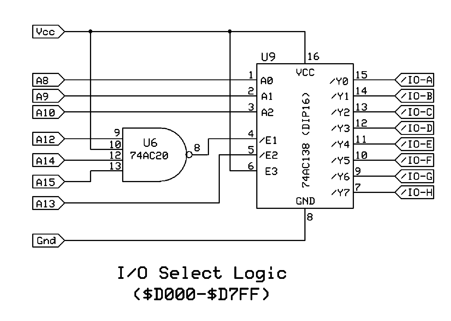
A little study of my design showed that with some judicious cutting and patching, I could use apply the above rules to qualify I/O accesses, which would fix the problem. Here's is what the I/O select logic looked like as designed:

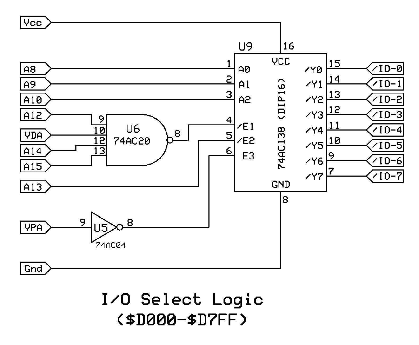
In the above arrangement, the 74AC138 decoder is being selected any time the expression A15 & A14 & !A13 & A12 is true, which is any address in the range $00D000 to $00DFFF. The problem is, of course, that the decoder is selected without regard to the validity of the address bus, as described in the above table. The decoder itself doesn't care, as it is very fast, and won't get confused by a false address bus state. However, if the expression A8 & !A9 & !A10 is also true when the decoder is selected, the DUART will be selected as well (/IO-B will be negated), again without regard to the validity of the address bus. To rectify this error, I changed the decoding logic to include VDA and VPA:

In the revised circuit, the MPU's VDA output is used to qualify the operation of U6 so its output stays high when A15 & A14 & !A13 & A12 is true during an invalid memory cycle. Further qualification with the MPU's VPA output prevents selection of any I/O device during a memory cycle in which the MPU is fetching an opcode or an operand. Hence the only time any I/O device will be selected is when A15 & A14 & !A13 & A12 is true and the MPU is reading or writing data. The resulting DUART select equation becomes:
A15 & A14 & !A13 & A12 & !A10 & !A9 & A8 & VDA & !VPAI inhibited I/O selection during the opcode and operand fetch memory cycles because it isn't expected that valid program instructions would come from an I/O device. I know: picky, picky!
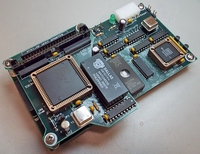
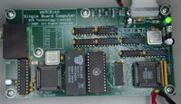
Making this change in the actual circuitry required the use of some wire-wrap wire and careful soldering, as well as cutting some chip legs. Here's what POC looked like after being patched to the new circuit:
Not visible in the photo are some of the cut chip legs. It was necessary to run the patch connections around the board edge because, being a four-layer board, it wasn't possible to drill through it to achieve a more favorable routing for the wires.
After verifying that POC would boot following the surgery, I tried out the indexed method of configuring the DUART, which now worked as it should. Feeling bold, I removed the 2 MHz oscillator from the Ø2 clock generator socket and installed a 16 MHz oscillator, which would result in an 8 MHz Ø2 clock. POC booted and appeared to operate normally. The eight-fold increase in the Ø2 clock rate was quite noticeable, especially in IRQ processing, which gets fairly intense during output to the console. After 'scoping some signals to see if anything hinky was occurring with the higher clock rate, I decided to let POC run without any user activity to verify stability. A few days later, I checked back on it—everything appeared to be copacetic. I had achieved a goal stated at the beginning of this diatribe: stable operation at 8 MHz.
Having put this hardware bug to bed I was able to resume firmware development.
Previous Page Home Next Page
Copyright ©1996–2026 by BCS Technology Limited. All rights reserved.
Unauthorized copying or reproduction of website content is prohibited.

