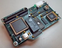
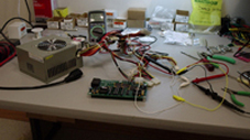
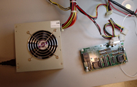
I started by removing all chips that were socketed, as well as the two clock oscillators—the only silicon left on the board was the SRAM and glue logic. The idea was to avoid damaging the "expensive" stuff in the event a serious circuit error put power where it didn't belong. It should be noted that PC power supplies are capable of producing copious amperage, certainly more than enough to turn chips into crispy critters if something goes awry. If the load is sufficiently severe the power supply will "crowbar" and immediately cut off output. However, that would still produce high current flow for a fraction of a second, more than enough time to take out something.
|
| Initial Test Setup — Click on Images to Enlarge |
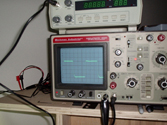
The application of power was uneventful. The "power good" LED illuminated and some poking around with both the meter and logic probe indicated that things were okay so far. Next I tried powering it with the two clock oscillators installed. My ancient Beckman dual-trace oscilloscope indicated that the Ø2 clock oscillator was running and that the clock generator flip-flip was producing an output.
A check of the DUART's baud rate clock generator showed that it too was working. Incidentally, that old Beckman 'scope in the above picture has a 20 MHz bandwidth, which is why the Ø2 signal isn't a pristine square wave. The el cheapo test probe I was using didn't help any.
Lastly, I metered the charge pump outputs on the MAX-238 TIA-232 transceiver and found the voltages to be in range. Just to satisfy myself that the transceiver would work, I attached my ancient TIA-232 diagnostic device to both ports and got the correct indications. With all of these preliminary steps completed, the next step would be to plug in the remaining chips and see if the thing would actually compute. There was no reason to think it wouldn't.
In order to determine if the MPU was running I would need to have it execute some instructions while monitoring the address and data buses for signs of activity. There are two ways to go about providing test code: a NOP generator plugged into the ROM socket or an actual ROM that has been loaded with a simple program. I decided to go with the latter and prepared three ROMs, one for the initial test, a second one to do some read/write operations on RAM and a third to do some read/write operations on the I/O hardware. The code in the first ROM was minimal:
$00E000 4C 00 E0 JMP $E000The endless branching back to $E000 would cause both address and data bus activity that could be monitored with the logic probe. Initially, I would watch A0, A1, A13, A14 and A15, since the above program should cause the MPU to repeatedly assert those lines as it fetched the opcode from the ROM. I'd also see activity on D0-D7 as the MPU first fetched the opcode and then the operand. If I did see such activity then it was an indication that the MPU was probably upright with a pulse and POC V1 was operational.
Operation with the first ROM demonstrated that there was MPU activity—all observed bus signals were active. Operation with the second ROM was likewise successful. The code in this one was a little more elaborate:
$00E000 A2 00 LDX #$00Here I also watched the /WD signal, which should be pulsing on each write cycle (STA $00,X), but only when Ø2 is high. Its action showed that the read/write logic was correct. This is where a dual-trace 'scope comes in handy: one channel was watching Ø2 and the other watching /WD. Also, I was using Ø2 to trigger the 'scope. A check of the SRAM's /CE input showed that it was being selected when it was supposed to be. Also, all data lines were pulsing as the program wrote successively larger values into each RAM location. So far, so good!
$00E002 8A TXA
$00E003 95 00 STA $00,X
$00E004 D5 00 CMP $00,X
$00E006 E8 INX
$00E007 80 F8 BRA $E002
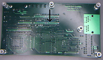
The third ROM was similar to the second except it was accessing one of the read/write configuration registers in the DUART. After a quick check to make sure the MPU was running I probed the /CEN (chip enable) input on the DUART to verify that it was being selected. It was continuously high, not good! It should have been pulsing. /CEN is driven by the /IO-0 output of the 74AC138 decoder, and like /CEN, /IO-0 was continuously high. That meant either the 'AC138 was defective or was not being enabled when it should be. I decided to pursue the latter case, since the days when chip defects were common are long gone. A quick check with the logic probe confirmed what I had suspected. During the PCB layout I somehow missed connecting A12 to pin 9 of U6, which is a quad-input NAND gate. With A12 not present, the gate wasn't driving the /E1 (enable) input of the 'AC138, so the decoder wasn't being enabled when any address in the $Dxxx range was being emitted by the MPU. A short piece of wire-wrap wire took care of the problem (see below—black arrow points to patch).
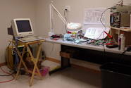
Now the DUART's /CEN input was pulsing, as was its /RDN (read enable) and /WRN (write enable) inputs. With these signals acting as they should, I had proved that all basic logic functions were working and that the MPU could access RAM, ROM and I/O. Now I needed to get the unit to drive the console terminal. Here's a picture of my augmented test setup:
Yep! That's a TV tray on which the WYSE 60 terminal is sitting. A little wobbly, but perfectly adequate. Also, note the ancient RS-232 tester hooked up to the terminal—it's that gadget attached to the blue ribbon cable that's resting on the keyboard. I had it there just in case something hinky occurred with the serial interface.
However, before I could try out POC V1 I had to cobble together enough code to perform a basic POST (power-on self-test), configure the I/O hardware and produce a display. I started with a very simple ROM that did little more than initialize the stack pointer, load some configuration values into the DUART and write the byte $41 to the DUART's channel–A TxD (transmit) register, which should display the letter A on the terminal screen. As I had prior experience with the DUART's big brother, the SCC2698 OCTART (functionally four DUARTs in one chip), no learning curve was required to write a simple DUART driver. Like its predecessors, this ROM used the MPU's emulation mode, which is the default at reset—I didn't want to introduce too many things to go wrong into this first effort.
I plugged the ROM into POC V1, powered everything, and the letter A appeared. My very first scratch-designed and built computer was functional! To say I was pleased that it worked on the first try would be an understatement. Given all that could go wrong, I was ecstatic, actually.
The next ROM, still operating in emulation mode, had a more elaborate POST screen driven by interrupts, along with a simple "TV typewriter" loop to verify that two-way TIA-232 communications were working. It took several days to write the code and visually verify the logic, which also included a rudimentary memory test. I tested some parts in the Kowalski simulator to avoid having to try to debug the ROM in the event it failed to produce the desired results. Finally, on December 27, 2009, the ROM was ready. I powered everything and was greeted with the following display:
Once the above had appeared, I type a few characters and saw that my typing was being echoed to the screen, demonstrating that bi-directional, interrupt-driven serial I/O was working. To quote my friend Lloyd Sponenburgh, who replied when sent the above picture via E-mail, "IT'S ALIVE!!!!"
Having leaped over the initial hurdle of getting POC V1 into operation, I went to work in developing more elaborate firmware, including code to detail-test memory at boot time, and cause the watchdog timer to generate jiffy interrupts and maintain a 32 bit uptime counter. I also wanted to see if I could design a fancier POST screen using the terminal's block graphics capabilities. Along the way, I ran into an interesting hardware bug (mentioned earlier on the system design page) that resulted in several pages of discussion on the 6502.org hardware forum.
Previous Page Home Next Page
