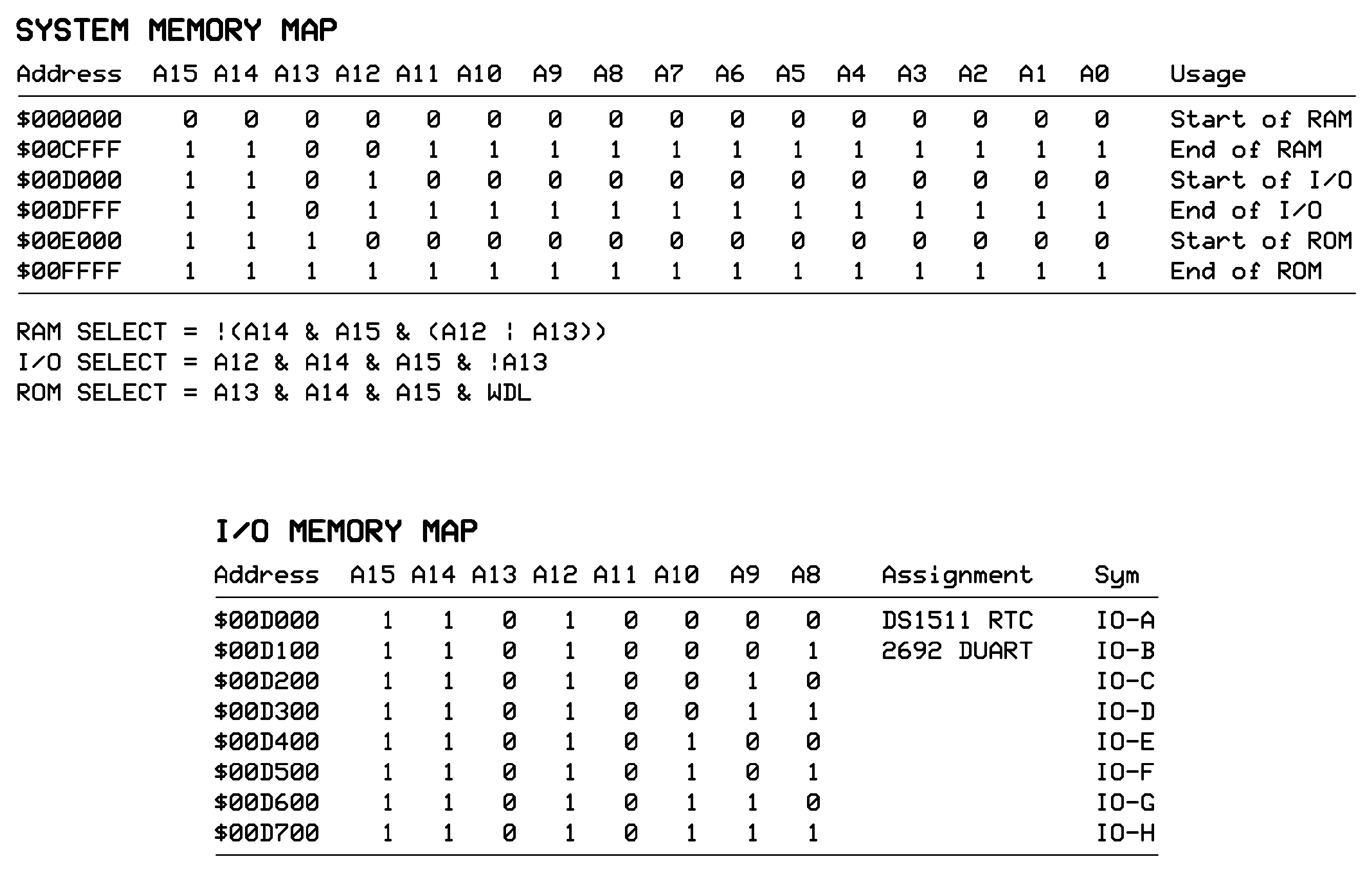
Note that I also expressed logic equations so I could relate the address bus bit patterns with what would actually happen in the circuit. In the logic equations, the symbol & means logical AND, | means logical OR and ! represents logical NOT (inversion). Also, note that one of the logic equations references a signal called WDL. WDL is true when the MPU is writing data—that is, when the MPU's RWB output is low, WDL is high. Hence ROM will not be selected if a write operation occurs to any address in the range $00E000-$00FFFF. Also note that I/O decoding occurs in one page (256 byte) segments, as I previously described. This obviously wastes some address space, but is not a concern. Decoding to a smaller address range per I/O device would greatly increase the amount of glue logic needed, but would not accomplish anything of value in return.
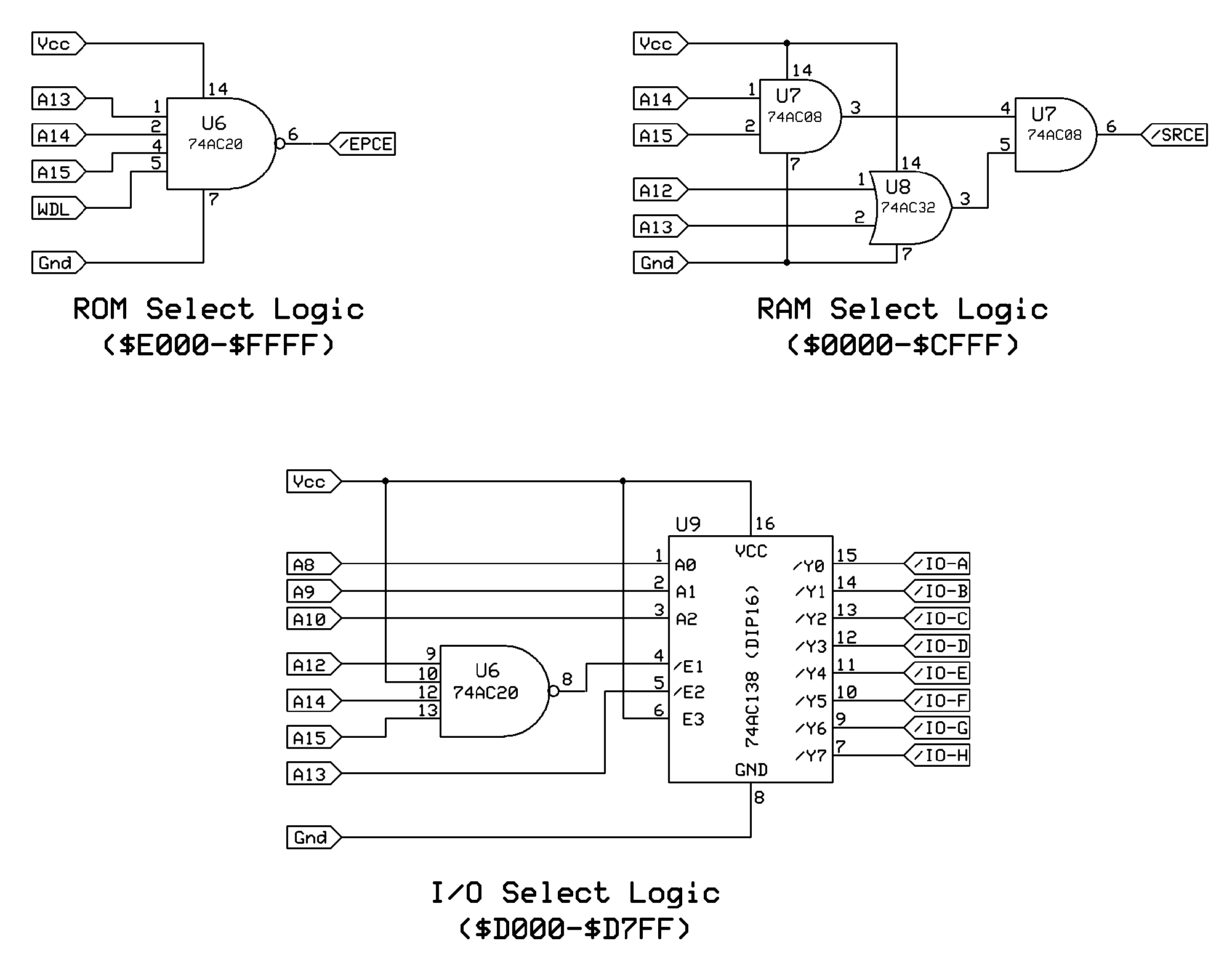
With the above information I could then work out how the glue logic would be interconnected to produce the desired results:

By way of explanation, the /EPCE signal (where the symbol / means active low), when true, selects the EPROM and /SRCE, when true, selects the SRAM. Note that no more than two gate delays are between the address bus and any one of the devices. It is understood that the amount of propagation delay that occurs in logic devices sets a hard limit on just how fast any system can run with reliability. By minimizing the number of gates involved, as well as using the fast 74AC logic, I was able to devise a glue logic setup that could, on paper, handle a 20 MHz Ø2 clock, even though such a clock rate wasn't practical with the chosen I/O hardware.
Incidentally, there's a bug—an error of omission—in the I/O select logic, which I'll explain when I get to how the circuit performed during initial testing.
Following the development of the glue logic, I drew a complete schematic of the unit. As I was using Express PCB's free-for-downloading software, I had a reasonably good electrical CAD program at my disposal. This CAD program can export its netlists to the board layout program included in the software, a feature which aids in correctly "wiring up" things. The schematic editor program isn't as powerful as a full commercial package, but it is more than adequate for hobby and light commercial work. The editor can also work with multiple sheets in one file, a feature that is essential for any project with any kind of complexity.
Here's the schematic I devised for my first-generation POC. Click on each image to enlarge it in a separate browser window:

Page 1: Memory Map |

Page 2: MPU Interface |

Page 3: RAM, ROM and I/O |
Not shown is page five, which is the parts list.
As can be seen, it's not a complicated design—pretty basic, in fact. However, it's enough to make a functional computer.
There are some design features worth noting:
- As mentioned before, the Ø2 clock signal is produced by
feeding the output of an HCMOS oscillator into a flip-flop.
The rise and fall time of a 74AC flop is extremely short, and
owing to the way flops work, the resulting output is almost perfectly
symmetric.
Since a D-type flop generates one output transition for every two
input transitions, Ø2 is one half the oscillator's frequency.
- Unused gates have their inputs tied to ground. Allowing a CMOS gate's input to float can result in the production of noise that can trigger instability, as well as result in a sharp increase in current consumption. A better way to terminate unused inputs is to pull them up to Vcc (5 volts) with resistors. Such an arrangement would allow the unused input to be used in the future if needed. However, the resistors would use up valuable printed circuit board real estate, which was a concern—surface area can account for a significant part of PCB manufacturing cost and I wanted to stay within the limits of EPCB's "ProtoPro" service, which I'll discuss in the next page.
- Ø2 is used to qualify the "write data" signal (WDL) so it is true only when Ø2 is high. When Ø2 is low, the data bus either contains the RAM bank address (the currently unused A16-A23 address component) or random content. Hence writing while Ø2 is low may put invalid data into a chip, causing no end of grief. Despite this feature, the circuit as designed had a timing bug involving I/O operation that took some searching to locate. I'll describe this on a following page.
- The Dallas 1813 econo-reset responds both to an external device (e.g., reset push button) sinking the reset line or a change in the state of Vcc (the 5 volt power source). At power application, the 1813 will hold the reset line low until at least 150 milliseconds have elapsed after Vcc has stabilized, giving the MPU adequate time to complete its reset steps. Interesting note: the 1813 can also be used as a debouncer in circuits where relatively slow response is acceptable, e.g., push button operated. Second interesting note: the DUART requires an active high reset, which is why an inverter's input is wired to the 1813.
One of the members of the 6502.org microprocessor forum had encountered an interesting problem involving an apparently slow-starting clock oscillator that wasn't stabilized by the time the /RESET circuit was released following initial power-on. The result was that his system wouldn't boot at power-on, but would boot if the reset button was pressed after power was applied. His description of the problem led me to investigate ways to prolong the initial /RESET release delay from the default 250 milliseconds. What I did was add a series resistor to the DS1813's Vcc connection, along with a parallel capacitor. The resulting R-C time-constant delayed the rise of Vcc to the DS1813 for about one second, thus increasing the total elapsed time before the release of /RESET. This addition had no effect on the release time when /RESET was pulled low by a push button, since the capacitor would already be charged. I also included a jumper in the circuit to bypass the resistor in the event testing showed that the extra delay wasn't needed (it wasn't in this design).
- In this first design, the only interrupt sources are the DUART and RTC, so there is no need for interrupt priority circuitry. Having mentioned interrupt priority, I should also mention that the '816 has a useful output signal called VPB (vector pull), which goes low right at the point in the machine cycle where the '816 fetches a vector address following receipt of an interrupt. VPB can be used along with interrupt priority circuitry to point the MPU to the appropriate interrupt service routine (ISR) for each device by changing the vector address on the fly. Such a feature can reduce the complexity of the ISR, as well as latency, since the selection of the appropriate code for each possible interrupt source is made in hardware in a fraction of the time that would be required to "soft-vector" the MPU. However, we're back to the requirement of minimizing hardware complexity, so VPB is not used in this design and the ISR performs the task of prioritizing IRQs. In any case, priority encoders of the type that would be used to implement this feature are relatively slow devices (they have many gates). The time spent in logic delays would be as long as that spent by the MPU in figuring out which device interrupted via software.
While bloviating about interrupts, I should mention that the physical interconnection of the interrupt circuitry is one of those design areas where a lack of understanding can lead to a lack of operation. The MPU has a single, active low interrupt request (IRQ) input (IRQB), which must be shared by all devices that use interrupts, using a circuit configuration called wired-OR. In my design, this circuit is designated /IRQ, which is pulled up to Vcc by a resistor that is part of resistor network RN1 (see schematic page 2 above), a pull-up resistor being a necessary feature of a wired-OR circuit. When /IRQ is released by the interrupting device, distributed capacitance in the circuit, which was discharged to ground while /IRQ was held low, has to be recharged to Vcc through the pull-up resistor. Hence this circuit has an R-C time constant, which means that a small but measurable amount of time is required for /IRQ to return to a high enough voltage to stop interrupting the MPU. If that time is excessive, /IRQ may not completely clear before the ISR has returned control to the interrupted task, resulting in a "phantom" or spurious interrupt that can cause all sorts of weird problems that will defy solution. Avoiding this sort of design problem is accomplished by careful board layout, proper component choices, and by clearing all interrupt sources as early as possible in the ISR.
- Although the SRAM (static RAM) has 128 KB of storage, only the first 64K are wired into the circuit, and only 52K are actually exposed to the '816. I used this particular SRAM because it was the smallest (capacity-wise) I could readily obtain whose access time was fast enough to support a wide range of Ø2 clock rates. These types of SRAMs are mostly produced in SMT packages, which adds to the challenge of constructing the computer—the pins are on 50 mil centers instead of the 100 mil centers of a standard DIP package. Keen eyes and a steady hand help while soldering. I'll discuss this aspect of construction on a following page.
Incidentally, SRAM is the preferred choice for homebrew computers. The alternative, DRAM (dynamic RAM), requires that refresh circuitry be implemented, which adds a fair amount of complexity to the system. Also, accessing DRAM is slower and more involved, characteristics that increase the likelihood of obscure timing problems. SRAM is much more expensive than an equivalent amount of DRAM, but is much easier to use.
- The two TIA-232 output jacks are wired to conform with the scheme that is used with Equinox SuperSerial TIA-232 multiplexers. As my UNIX software development system's hardware includes an Equinox SST16 unit, using this wiring scheme simplified the interfacing of the POC to the UNIX box, as well as to the WYSE 60 terminal whose modular adapter was already wired to interface to Equinox hardware. In addition to the required Gnd (ground), RxD and TxD signals, I implemented CTS and RTS so I could use hardware handshaking. Generally speaking, software handshaking (aka XON/XOFF handshaking) is unreliable above 9600 bits per second (bps). I did not incorporate any XON/XOFF code into the BIOS, relying solely on CTS/RTS.
- Speaking of TIA-232, the inputs and outputs of the DUART are TTL-level signals, whereas the equivalent TIA-232 signals swing (more-or-less) between plus and minus 12 volts DC. The voltage level conversion is performed by a Maxim MAX-238 transceiver, which is functionally equivalent to two MAX-232 transceivers in a single package. An alternative choice would have been to use 1488 and 1489 line drivers. The MAX-238, while much more expensive (in relative terms) than the line drivers, uses a lot less board space (it's in a DIP24 package and is also available in SOIC-24) and only requires a single 5 volt DC power source. If I had instead used the 1488 and 1489 I would have had to provide plus and minus 12 volts to feed them, as well provide the 5 volts (Vcc) that powers everything else, not to mention find room for them on the PCB. Again, simplicity was the paramount factor in this choice.
- I was liberal with the use of decoupling capacitors. CMOS logic devices often generate large transients as they switch between logic states (especially at elevated clock rates), and thus tend to introduce noise into the circuit. More than a few homebrew computer designs have been victims of unacceptably high noise levels, preventing operation at anything other than a low clock rate akin to that of a cheap pocket calculator. Decoupling capacitors are quite inexpensive and consume little space on the board, so don't be afraid to use plenty of them in your project. I use the X7R series for best performance.
Previous Page Home Next Page

